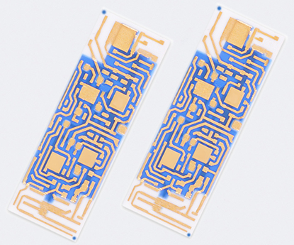
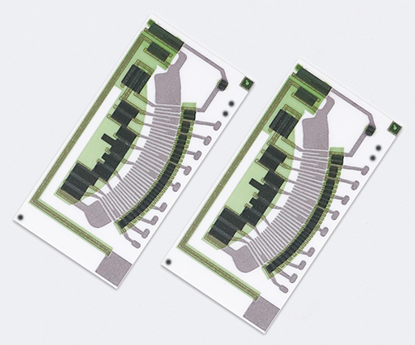
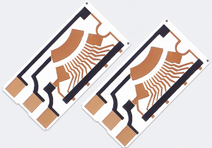
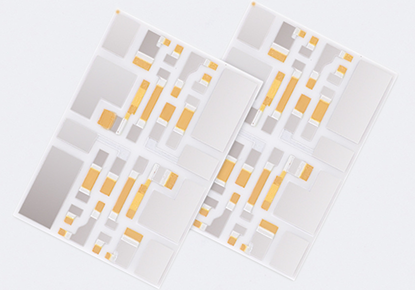
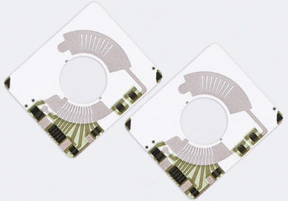
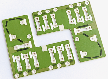
Thick Film Circuits
Thick Film Circuits are robust electronic circuits formed by applying conductive, resistive, and insulating materials onto ceramic or other substrates using a thick film printing process, followed by high-temperature sintering to ensure durability, reliability, and resistance to environmental factors like temperature fluctuations and mechanical stress, offering the ability to customize resistance values, sizes, and power handling, making them well-suited for demanding applications in industries such as automotive, aerospace, medical devices, and telecommunications. Thick Film Circuits offer versatility and reliability by integrating conductive, resistive, and insulating materials on a single ceramic substrate. They are highly resistant to high temperatures, humidity, and mechanical stress, making them ideal for harsh environments. Cost-effective by reducing wiring and assembly needs, these circuits lower production costs while ensuring precise and durable components. Thick Film Circuits are used across industries requiring performance, durability, and compactness, such as automotive electronics, medical devices, telecommunications, and industrial control systems. In automotive applications, they are found in engine control units and sensor systems. In medical devices, they provide precision and resistance to external factors. They are also essential in telecommunications for signal processing and in industrial control systems for automation and machinery reliability. Main Features of Thick Film Circuits : |
 |
|
 |
1, Reliability: Thick Film Circuits demonstrate good electrical performance and long-term reliability. Their stable characteristics make them suitable for applications that require consistent performance over extended periods. 2, Robustness: Thick film materials, once processed and cured, exhibit excellent physical and chemical stability. They can withstand high temperatures, moisture, and mechanical stress, making TFCs suitable for harsh environments and demanding applications. 3, Compactness: Thick Film Circuits enable the creation of highly compact circuits with minimal space requirements. The ability to print layers of conductive and resistive materials onto a substrate allows for the dense integration of components and interconnects. |
|
4, Integration: Thick Film Circuits can easily integrate with other components, such as capacitors, inductors, and sensors, enabling the development of functional circuits with improved performance and functionality. 5, Hybrid Circuits: A significant portion of thick film circuits are used as the basis for hybrid circuits, which combine thick film technology with other types of microelectronic components. 6, High-Frequency Capability: While primarily used in lower frequency applications, TFCs can also be designed to operate at moderate frequencies, making them suitable for certain RF (radio frequency) applications. |
||
 |
7, Cost-effective: Thick Film Circuits offer a cost-effective solution compared to other circuit technologies like thin film or printed circuit boards. The materials used in TFCs, such as thick film pastes, are relatively inexpensive, and the manufacturing processes, such as screen printing, are efficient and affordable. 8, Customization: Thick Film Circuits offer flexibility in circuit design and customization. The screen printing process allows for precise patterning and adjustment of component values, such as resistance values, to meet specific requirements. 9, Versatility: Thick Film Circuits can be fabricated on a wide range of substrates, including ceramics, glass, and flexible materials. This versatility allows for the integration of TFCs into different types of devices and systems. 10, Microwave Properties: Thick film circuits are designed with thermal management and microwave properties in mind, which are crucial for their performance in various applications. |
|
Thick Film Circuits based on Thick Film Technology make them a preferred choice in various industries and applications, including automotive, medical, industrial, and consumer electronics. Their cost-effectiveness, compactness, and reliability contribute to their popularity as a circuit technology. Please refer to Thick Film Technology for more informations. |
||
Applications of Thick Film Circuits : |
Thick Film Circuits are created by printing conductive, dielectric, and resistive materials onto a substrate, followed by a sintering process to form the circuit. Due to their unique manufacturing process and excellent performance, thick film circuits are widely used in various fields. Below are some of the main applications: 1. Electronic Components: ● Capacitors, Diodes, Sensors: Thick film technology can also be used to manufacture integrated electronic components such as capacitors and diodes, especially in circuits that require miniaturization and high density. |
|
 |
2. Automotive Electronics: ● Sensors and Detection: Thick film circuits are also used in various automotive sensors, such as temperature sensors, oxygen sensors, and pressure sensors, which help monitor and control vehicle performance. 3. Industrial Control: ● Process Control Instruments: Thick film circuits are used in measuring and controlling process variables such as temperature, humidity, and pressure, making them suitable for operation in harsh industrial environments. |
4. Medical Electronics: 5. Aerospace: ● Inertial Navigation Systems: In aerospace applications, thick film sensors are used in inertial navigation systems, capable of withstanding high levels of radiation and temperature fluctuations over long periods. 6. Optoelectronics and Laser Technology: ● Optical Sensors: Thick film circuits are used in optoelectronic applications, such as optical sensors, to monitor light signals and perform signal processing. |
|
 |
7. Communication Equipment: ● Satellite Communication and Radar Systems: Thick film circuits are also used in satellite communication equipment and radar systems, where high-density, anti-interference, and excellent thermal stability are critical. 8. Consumer Electronics: ● Mobile Phones and Portable Devices: In some small, low-power electronic devices, TFCs help increase circuit density, reducing the amount of space needed. |
9. Military and Defense: ● Electronic Warfare Equipment: In electronic warfare, thick film circuits are used in high-frequency, low-temperature, and anti-jamming circuits, ensuring the reliability of electronic warfare equipment. 10. Energy Sector: ● Battery Management Systems: Thick film circuits are used in battery management systems (BMS) to monitor and manage batteries, ensuring safety and long lifespan. |
|
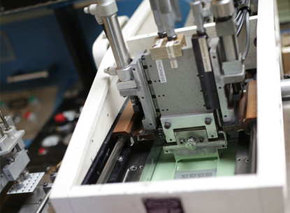
Manufacturing Processes of Thick Film Circuits : |
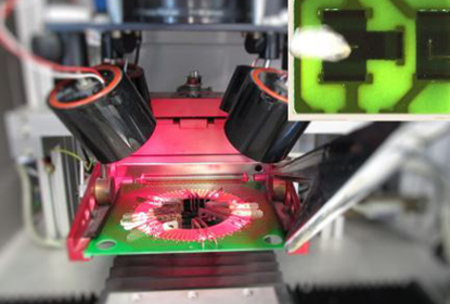
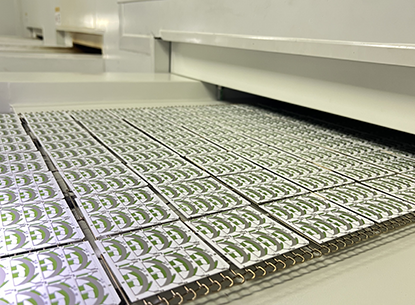
1, Substrates Selection: Thick Film Circuit materials are applied onto ceramic substrates, such as alumina (Al2O3), beryllium oxide (BeO), and aluminum nitride (AlN). This ceramic substrate is the base-plate for the hybrid circuits on which the different layers are applied. The ceramic substrate can also be substituted with different types of materials depending on the application requirements. 2, Screen-Printing: All of the electrical traces (conductive, resistive, dielectric) are formed by screen-printing process onto the ceramic substrate. The screens themselves are produced by a photomasking technique or laser cutting process,We called it as "Printed stencil",where exposure to UV light selectively hardens coated regions, after etching process leaving “holes”, where the screen printing machine squeegee pushes the pastes through and onto the ceramic. |
|
 |
3, Drying and Baking: Thick Film Circuits screen-printed onto ceramic subtrate are then Pre-dried in an oven at 200°C before being baked at around 850°C. Additional layers (conductive layer, resistive layer, dielectric layer) are added by making repeat passes through the screen-printing, drying and baking processes. Other functional elements when fired, like dielectrics, are a mixture of glass and specific ceramics that do a combination of melting and dissolving into each other to form a new material during the firing process which generates specific characteristics. 4, Multilayer Hybrid Circuits: The additive screen-printing process can be repeated multiple times using dielectric material (protect layer) to insulate the conductor. Additional metal and dielectric layers can be added thus achieving a multilayer structure. The small openings called vias in the dielectric layers are filled with metal thus connecting various circuit lines to corresponding circuit lines above or below the layer. |
5, Laser Trimmed: One special feature of thick film circuits manufacturing is the ability to screen-printing the resistors along with the others electrical traces. But, screen printed resistors by normal process will be with a value tolerance about +/-20%,In this case, We can use laser trimming to reduce variability to better than +/-1%, In laser trimming each resistor is probed to measure its actual resistance, If below the nominal or target value a laser then selectively removes resistive material to reduce the area through which current flows, thereby increasing the resistance. 6, Holes Metallization: Thick Film Circuits using various metals can barrel coat and plug holes that are drilled though the ceramic substrate. When incorporating metallized through-holes in a design, the opposite side of the board can act as a separated or connected circuit. PTH with metallization connections can be used to integrate various other conductor layers which is a major advantage when the circuit density requirement is very high. |
|
Advantages of Thick Film Circuits : |
1, Low CTE: Thick Film Circuits has solid and outstanding interatomic bonds, so Thick Film Circuits can withstand high temperatures and is still firm, stable, and steady even under changing temperatures. 2, Excellent Thermal Insulation: Thick Film Circuits is incredibly insulating; therefore, heat will be less likely to flow through the substrate, preserving the ceramic hybrid circuit's components from getting damaged or harmed. |
|
 |
3, Space efficiency: Thick Film Circuits allow for the creation of highly compact circuits. The ability to print layers of conductive and resistive materials onto a substrate enables the dense integration of components and interconnects. This compactness is particularly advantageous in applications where space is limited or miniaturization is required. 4, Long Term Reliability: Most commercially packaged semiconductors will have a life span measured in years, while hybrids have a life span measured in decades. 5, Design flexibility: Thick Film Circuits allow for great design flexibility. The screen printing process used in TFC fabrication enables precise patterning and customization of circuits. Components, interconnects, and resistors can be easily adjusted, resized, or modified to meet specific circuit requirements. This flexibility makes TFCs suitable for a wide range of applications. |
6, High Thermal Conductivity: When electronics operate at elevated temperatures the materials used can have a substantial impact on performance and life. With its ability to dispel heat, ceramic substrate performs better and can prevent a device from being damaged by high temperatures. Depending on the material used, like Alumina or Aluminum Oxide, Aluminum nitride (AlN), beryllia or beryllium oxide (BeO), silicon carbide (SiC), and boron nitride (BN), the values range from 20 to 300 W/(m·K). 7, Multi-Layering: A multi-layer hybrid circuit can do a more complicated task. With the toughness of its material, another layer can be added easily and still keep the other components safe. Ceramic hybrid circuit is excellent for heavy-duty applications. |
|
 |
8, Integration capability: Thick Film Circuits can easily integrate with other components and technologies. They can be combined with passive components like capacitors and inductors, as well as active components such as sensors and semiconductors. This integration enables the creation of complete functional circuits with improved performance and functionality. 9, Custom Packaging: Thick Film Circuits, or custom monolithic IC packages, provide flexibility for shape and package style, as well as the option for improved performance. 10, Wide application range: Thick Film Circuits find applications in various industries and technologies. They are used in automotive electronics, industrial controls, medical devices, consumer electronics, telecommunications, and more. Their versatility and suitability for different environments and requirements make TFCs a preferred choice for diverse applications. |
11, Low Failure Rate: Aside from long term reliability, Thick Film Circuits also exhibit a lower mean time between failure rate when exposed to environmental stresses such as high temperature, mechanical vibration or other harsh conditions. The Advantages of Thick Film Circuits, including cost-effectiveness, design flexibility, integration capability, compactness, reliability, quick prototyping, and good electrical performance, make them a popular and practical circuit technology in numerous industries. |
|
Why Deed to Customize Thick Film Circuits ? |
1, Tailored Performance: Customization enables engineers to optimize the performance of thick film circuits to suit specific application requirements. This involves tailoring parameters such as electrical characteristics, thermal properties, and signal processing capabilities to achieve desired performance metrics, such as speed, accuracy, and efficiency. 2, Space Optimization: Custom Thick Film Circuits can be designed to fit within constrained spaces or conform to irregular shapes within a device or system. This space optimization is particularly crucial in compact electronic devices where minimizing footprint is essential for efficient integration and functionality. |
|
 |
3, Enhanced Functionality: By customizing the circuit layout and component selection, designers can enhance the functionality of thick film circuits to support advanced features. This may involve incorporating additional sensors, communication interfaces, or signal conditioning circuits to meet specific application needs. 4, Improved Reliability: Customization allows for the selection of materials and manufacturing processes optimized for reliability and durability in challenging operating environments. This includes choosing robust substrate materials, protective coatings, and soldering techniques that enhance resistance to temperature variations, humidity, vibration, and other environmental factors. 5, Cost Efficiency: While customization may involve initial design and setup costs, it can lead to long-term cost savings by optimizing performance, reducing material waste, and streamlining production processes. |
6, Integration Flexibility: Customization facilitates seamless integration of thick film circuits with other system components or modules, enabling enhanced functionality and system-level optimization. This integration simplifies assembly processes, reduces interconnect complexity, and enhances overall system reliability and performance. Custom Thick Film Circuits allows for tailoring their performance, size, functionality, reliability, and cost-effectiveness to specific application requirements. This customization ensures that the circuits meet the unique needs and challenges of diverse electronic systems and devices, ultimately contributing to their efficiency, effectiveness, and competitiveness in the market. |
|
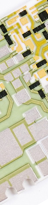
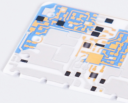
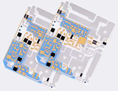
Typical Stack-Up of Thick Film Circuits : |
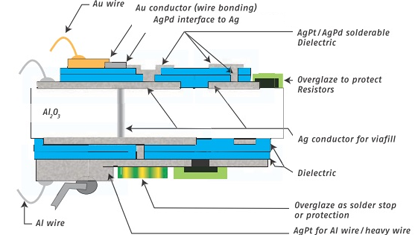 |
1, Substrate: The base material on which the thick film circuit is built. Common substrate materials include alumina, aluminum nitride, and beryllium oxide. 2, Conductive Layer: This layer consists of a thick film paste made of conductive materials such as silver, gold, or palladium. The paste is screen-printed onto the substrate to create the circuit pattern. 3, Dielectric Layer: A layer of thick film dielectric material is applied over the conductive layer to provide electrical insulation and protection. 4, Resistive Layer: In circuits with resistive elements, a resistive layer made of a specific thick film paste is added to create the required resistance values. 5, Protective Layer: A final layer of protective material, such as glass or a conformal coating, is applied to safeguard the circuit from environmental factors and damage. |
Manufacturing Challenges of Thick Film Circuits : |
Manufacturing Thick Film Circuits involve several challenges and hurdles across various stages of production, from material selection to the printing of multilayer circuits. Here is a comprehensive overview of the manufacturing challenges and obstacles faced in the production of thick film circuits: |
|
 |
1, Material Selection: 2, Production Processes: |
3, Firing Process: 4, Multilayer Circuit Printing: |
|
 |
5, Alignment and Registration: 6, Via Formation: |
7, Metallization Challenges: 8, Etching and Trimming Difficulties: The production of Thick Film Circuits poses challenges across material selection, production processes, multilayer printing, firing, metallization, etching, and trimming. Overcoming these challenges demands careful attention to detail, precise control of process parameters, and the implementation of quality assurance measures to ensure the reliability and performance of thick film circuits in various electronic applications. |
|
Why Choose PANDA PCB For Thick Film Circuits ? |
PANDA PCB Group ’ Thick Film Circuits provided superior circuit density, performances, and reliability, with relatively low development and tooling costs. Our highly skilled and motivated engineering team uses the best and brightest thinking to develope production processes for customers in the field of the medical and industrial technologies. PANDA PCB provided over 20 years of experience in the design and manufacture of Thick Film Circuits for high-reliability application in the industrial, medical, and military markets. Our superior-quality manufacturing process is certified according to ISO9001, ISO14001 and IATF 16949. |
||
 |
At PANDA PCB Group 's Thick Film Circuits, We provide thick film circuits manufacturing, soldered hybrids, through-hole metallizations in ceramics, bonding hybrids, multilayer circuits (up to 2 conductor layers per side), etc. That means, We can provide multilayer hybrid circuits up to 4-layers, which is a technique for further improvements in integration using a screen-printing insulating dielectric to ensure connections between layers are made only where required. On the basis of packaging type, the market for hybrid circuits has been segmented into hermetic packaging and non-hermetic packaging. By end-use industry, the market has been segmented into aerospace & defense, automotive, industrial, consumer electronics, healthcare power generation, oil & gas and others. The majority of the actual thick film circuit products are customized solutions designed to fit our customers specific requirements. By focusing on funded R&D projects in the field of micro systems and sensors, we are developing hybrid circuits in our future. |
|
Design Guidelines of Thick Film Circuits : |
We compiled a Thick Film Circuits-Design Guidelines as attached for you to download, It is to better support our customers' needs in designing and applying Thick Film Circuits, This guide covers detailed information on product solutions, engineering design specifications, material properties, available manufacturing processes, and more. We hope that this guide will assist customers in standardizing their design process while ensuring the manufacturability of the design data, ultimately improving product reliability and production efficiency. Customers are encouraged to refer to the guide when designing Thick Film Circuits to ensure adherence to best practices. |
Capabilities of Thick Film Circuits Are As Follows : |
1, Optional Processes of Thick Film Circuits :
Metalization Types : |
Thick Film Substrates (Screen-Printed) |
Thin Film Substrates (Photo-Imaged) |
|||
Process Types : |
TFM Capabilities |
HTCC / LTCC Capabilities |
DBC Capabilities |
DPC Capabilities |
AMB Capabilities |
Layer Counts : |
1, 2, 3, 4, 5, 6 Layers |
1, 2, 4, 6, 8, 10, 12 Layers |
1, 2 Layers |
1, 2 Layers |
1, 2 Layers |
Max Board Dimension : |
200*230mm |
200*200mm |
138*178mm |
138*190mm |
114*114mm |
Min Board Thickness : |
0.25mm |
0.25mm |
0.30mm~0.40mm |
0.25mm |
0.25mm |
Max Board Thickness : |
2.2mm |
2.0mm |
1L: 1.6mm; 2L 2.0mm |
2.0mm |
1.8mm |
Conductor Thickness : |
10um - 20um |
5um - 1500um |
1oz - 9oz |
1um - 1000um |
1oz- 22oz |
Min Line Width/Space : |
8/8mil (0.20/0.20mm) |
6/6mil (0.15/0.15mm) |
10/10mil (0.25/0.25mm) |
6/6mil (0.15/0.15mm) |
12/12mil (0.30/0.30mm) |
Substrates Types : |
AI203, ALN, BeO, ZrO2 |
AI203, ALN, BeO, ZrO2 |
Al2O3, AlN, ZrO2, PbO, SiO2, ZTA, Si3N4, SiC, Sapphire, Polycrystalline Silicon, Piezoelectric Ceramics |
Al2O3, AlN, ZrO2, PbO, SiO2, ZTA, Si3N4, SiC, Sapphire, Polycrystalline Silicon, Piezoelectric Ceramics |
AI203, ALN, BeO, ZrO2, Si3N4 |
Min Hole Diameter : |
4mil (0.15mm) |
4mil (0.15mm) |
4mil (0.1mm) |
4mil (0.1mm) |
4mil (0.1mm) |
Outline Tolerance : |
Laser: +/-0.05mm; Die Punch: +/-0.10mm |
Laser: +/-0.05mm; Die Punch: +/-0.10mm |
Laser: +/-0.05mm; Die Punch: +/-0.10mm |
Laser: +/-0.05mm; Die Punch: +/-0.10mm |
Laser: +/-0.05mm; Die Punch: +/-0.10mm |
Substrate Thickness : |
0.25, 0.38, 0.50, 0.635, 0.80,1.0, 1.25, 1.5, 2.0mm, Customizable |
0.25, 0.38, 0.50, 0.635, 0.80,1.0, 1.25, 1.5, 2.0mm, Customizable |
0.25, 0.38, 0.50, 0.635, 0.80,1.0, 1.25, 1.5, 2.0mm, Customizable |
0.25, 0.38, 0.50, 0.635, 0.80,1.0, 1.25, 1.5, 2.0mm, Customizable |
0.25, 0.38, 0.50, 0.635, 0.80,1.0, 1.25, 1.5, 2.0mm, Customizable |
Thickness Tolerance : |
0.25-0.38: +/-0.03mm; 0.50-2.00: +/-0.05mm |
0.25-0.38: +/-0.03mm; 0.50-2.00: +/-0.05mm |
0.25-0.38: +/-0.03mm; 0.50-2.00: +/-0.05mm |
0.25-0.38: +/-0.03mm; 0.50-2.00: +/-0.05mm |
0.25-0.38: +/-0.03mm; 0.50-2.00: +/-0.05mm |
Surface Treatment : |
Ag, Au, AgPd, AuPd |
Ag, Au, AgPd, AuPd, Mn/Ni |
OSP/Ni Plating, ENIG |
OSP/ENIG/ENEPIG |
OSP/ENIG/ENEPIG |
Min Solder PAD Dia : |
10mil (0.25mm) |
10mil (0.25mm) |
8mil (0.20mm) |
6mil (0.15mm) |
8mil (0.20mm) |
2, Engineering Specification of Thick Film Circuits :
Items : |
Typical Values |
Advanced Capabilities |
1, Substrates : |
FR4, Ceramic ( AI203, ALN, BeO, ZrO2), Polyimide (Flexible PI), Stainless Steel (SUS304), Mica |
FR4, Ceramic ( AI203, ALN, BeO, ZrO2), Polyimide (Flexible PI), Stainless Steel (SUS304), Mica |
2, Conductor (Paste) Materials : |
Copper, Silver , Gold , Silver-Palladium, Palladium-Gold, Platinum-Silver, Platinum-Gold |
Copper, Silver , Gold , Silver-Palladium, Palladium-Gold, Platinum-Silver, Platinum-Gold |
3, Thick Film Carbon Thickness (Height) : |
15um +/-5 um |
30um +/-5 um |
4, Conductor Thickness (Height) : |
12um+/-5um |
20um+/-5um |
5, Min Width of Thick Film Line : |
0.30 mm +/-0.05 mm |
0.20 mm +/-0.05 mm |
6, Min Space of Thick Film Line : |
0.30 mm +/-0.05 mm |
0.20 mm +/-0.05 mm |
7, Min Overlap (Carbon to Conductor) : |
No less than 0.25mm |
0.20mm (Minimum) |
8, Sheet Resistivity (ohms/square): |
Printed resistors in milli ohm to mega ohm range (Customizable) with tolerances of 1-10% are fabricated and protected with overglaze materials. |
Printed resistors in milli ohm to mega ohm range (Customizable) with tolerances of 0.5-10% are fabricated and protected with overglaze materials. |
9, Resistor Value Tolerance (ohms) : |
+/-10.0% (Standard) (Customizable) |
+/-0.5% (Laser trimming) |
10, Linearity : |
+/-1.0% (Standard) (Customizable) |
+/-0.2 ~ +/-0.5% (Laser trimming) |
11, Synchronism of Double Channels : |
+/-2.0% (Standard) (Customizable) (Potentiometers) |
+/-1.0% (Laser trimming) (Potentiometers) |
12, Durability of Carbon Ink (Life time) : |
0.5 Million (Min), 2.0 Million (Standard) |
5.0-10.0 Million (Max) with Surface Polishing |
13, Working Temperature : |
- 40ºC /+150ºC |
- 40ºC /+180ºC |
3, Optional Substrates of Thick Film Circuits :
Substrates : |
Alumina (Al2O3) |
Aluminum Nitride (AlN) |
Beryllium Oxide (BeO) |
Zirconium Dioxide (ZrO2) |
Max Application Temperature : |
662 - 1832 |
1832 |
2300 |
2432 |
Max Power Density (W/in²): |
75 |
1010 |
250 |
300 |
Max Ramp Up Speed (°F/sec): |
122 |
572 |
400 |
350 |
Thermal Conductivity (W/mK): |
20-35 |
180-220 |
200-300 |
2.0-5.0 |
Density (g/cm³): |
3.75 |
3.26 |
2.8 |
5.9 |
Dielectric Loss: |
0.0001 - 0.001 |
0.0001 - 0.0005 |
0.0001 - 0.0002 |
0.0005 - 0.001 |
Dielectric Constant: |
9.4 - 10.2 |
8.5 - 9.0 |
6.0 - 7.0 |
25 - 30 |
CTE, ppm/ºC: |
6.0 - 8.0 |
4.0 - 5.0 |
7.0 - 9.0 |
10.0 - 11.0 |
Substrate Thickness (mm): |
0.25 - 2.0 |
0.25 - 2.0 |
0.25 - 2.0 |
0.25 - 2.0 |
Typical Max. Dimension (inch): |
6 x 12 |
5 x 11 |
6 x 6 |
4 x 4 |
Theoretical Total Wattage (W): |
5400 |
55000 |
15000 |
20000 |
4, Conductive Paste of Thick Film Circuits :
Paste ( Materials) : |
Conductor Width/Space |
Soldering / Bonding |
Gold : |
8/8mil (0.20/0.20mm) |
Gold is a good conductor material and allows thermo-compression gold wire bonding and eutectic die attachment. It is, of course, costly and has poor solderability. |
Silver : |
8/8mil (0.20/0.20mm) |
Soldering & Silver is lower in cost, and solderable, but is not leach-resistant with tin/lead solders.More seriously, silver atoms migrate under the influence of DC electric fields, both causing short-circuits and reacting with many of the resistor paste formulations. |
Platinum-Silver : |
6/6mil (0.15/0.15mm) |
Soldering & Surface Mount, Palladium and platinum alloyed to the gold and silver produce good conductor pastes,with good adhesion to the substrate, good solderability, and moderately good wire bonding characteristics. Copper and nickel are examples of materials that have been proposed for paste systems as substitutes for noble metals. |
Palladium-Silver : |
8/8mil (0.20/0.20mm) |
Soldering & Surface Mount ,Solderable, Wire bondable, (good aged adhesion general purpose), Silver-palladium conductor inks are the most commonly used materials, with both price and performance (primarily resistance to solder) increasing with palladium content. |
Platinum-Gold : |
6/6mil (0.15/0.15mm) |
Soldering & Au or Al Wire Bonding, Solderable (excellent aged adhesion with no migration). |
Palladium-Gold : |
8/8mil (0.20/0.20mm) |
Soldering & Au or Al Wire Bonding, Wire bondable. |
5, Resistive Paste of Thick Film Circuits :
Performances : |
Common Values/Range |
Description |
Resistance Value : |
1Ω to several MΩ |
The resistance value depends on the type and ratio of carbon black, typically ranging from 1Ω to Mega ohm. |
Resistance Tolerance : |
±1% to ±10% |
High-precision resistors can achieve ±0.1% tolerance used laser trimming process. |
Temperature Coefficient (TCR) : |
±50ppm/°C to ±200ppm/°C |
High-quality resistive paste should have a low TCR, preferably below ±100ppm/°C. |
Stability : |
≤1% |
Resistors must undergo high-temperature aging and humidity tests to ensure stability. |
Sintering Temperature : |
850°C to 950°C |
The sintering temperature for carbon paste depends on material properties, typically in this range. |
Conductivity : |
10⁶ S/m to 10⁸ S/m |
Conductivity depends on the type and ratio of carbon black, affecting resistance precision and stability. |
Surface Smoothness : |
Ra≤ 1 μm |
The surface must be free of cracks, bubbles, and non-uniform layers to ensure good mechanical and electrical properties. |
Insulation Resistance : |
≥10⁹ Ω |
Carbon paste should have good insulation properties to avoid leakage or short circuits. |
Mechanical Strength : |
≥100 MPa |
The resistive layer must have good compressive and bending strength to ensure the reliability of the resistor. |
Volatility : |
Solvent residue ≤ 1% |
High volatility solvents help with even coating and drying, but excessive volatility may affect electrical performance. |
Oxidation Resistance : |
>1000 hours |
High-quality carbon paste should have strong oxidation resistance to extend the service life. |
Humidity Resistance : |
≥1000 hours |
Resistors should be able to withstand high-humidity conditions to ensure long-term stable performance, no significant changes. |
6, Dielectric Paste of Thick Film Circuits :
1, High Dielectric Strength: The paste should have a high dielectric strength to serve as an insulating layer between conductor layers in multilayer thick film circuits. 2, Excellent Insulation Resistance: When applied as a protective layer on conductor layers, the paste should exhibit good insulation resistance to prevent current leakage. 3, Low Power Factor: When used as an insulating layer for thick film heating elements on a metal core (e.g., stainless steel), the paste should have a low power factor to minimize energy loss. 4, Optimal Dielectric Constant: For thick film resistor elements, a high dielectric constant is advantageous. However, to ensure stability, the maximum achievable dielectric constant is typically around 10. Materials with higher dielectric constants may introduce thermal coefficient issues. 5, Low Thermal Coefficient: The paste should have a low thermal coefficient to maintain consistent properties and performance across a range of temperatures. 6, Suitable Viscosity: The viscosity of the paste should be appropriate for the printing process and desired layer thickness. It should flow easily during printing but not be too thin, preventing uneven coating or spreading. 7, Precise Curing Conditions: Proper control of curing conditions, including temperature and time, is crucial to achieving strong bonding and adhesion between the paste and substrate. 8, Compatibility: The paste should be compatible with other materials used in the circuit, such as conductor pastes and protective coatings, to ensure proper integration and avoid adverse reactions or changes in material properties. |
7, Insulating Paste of Thick Film Circuits :
1, Insulating paste for thick film circuits is a type of material used in the manufacturing of electronic circuits. It is applied to the surface of the circuit to provide protection from environmental factors such as moisture, dust, and other contaminants. This protective paste helps to ensure the reliability and longevity of the circuitry by safeguarding it from external influences that could cause damage or malfunction. 2, Commonly used non-metallic materials for protective coatings include overglazes (Glass-Glaze), enamel, polymers, and epoxies,depending on application conditions and environment. 3, The insulating-protective layer for custom heating element is printed or coated continuously to cover the heater assembly as the sheath of the heating element with several intents: mechanically protecting physical damage, electrically insulating the heating traces, preventing corrosion along with water resistance, thermally withstanding maximum application temperatures, against outgassing in high vacuum (Vacuum protection), and withstand high voltage. |