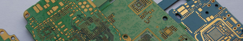
HDI PCB
HDI PCBs, also called High Density Interconnect PCBs, are cutting-edge printed circuit boards designed with an exceptionally high density of electronic components and interconnections, achieved through features like narrower trace widths, reduced layer spacing, and the incorporation of microvias, as well as blind and buried vias, enabling a significantly higher number of connections within a compact area, which not only facilitates the miniaturization of electronic devices but also improves signal integrity, minimizes power consumption, and enhances the overall reliability, performance, and functionality of devices. HDI PCBs offer significant performance and miniaturization advantages. By utilizing advanced manufacturing techniques, such as laser drilling, fine-pitch components, and stacked or staggered vias, HDI PCBs support high-speed, high-frequency applications. These boards are particularly well-suited for devices that require both compactness and high performance. Additionally, they ensure superior signal integrity and effective thermal management, making them indispensable in modern electronics that prioritize power and size efficiency. High Density Interconnect PCBs are widely used in high-performance applications where compactness and reliability are key. They are commonly found in smartphones, tablets, wearables, and other portable devices, as well as in medical devices, automotive electronics, and telecommunications equipment. With their ability to support complex designs and high-speed data transmission, HDI PCBs are also essential in emerging technologies like IoT devices, drones, and wearables, offering a perfect balance of miniaturization and performance. Key Features of HDI PCB : |
 |
|
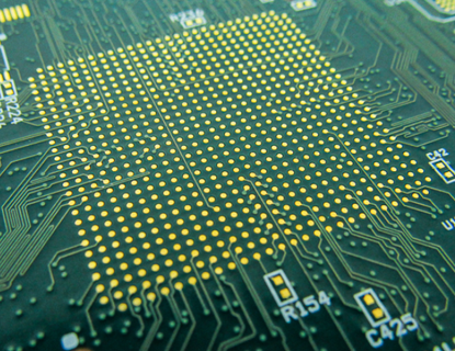 |
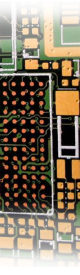
1, Microvias: HDI PCBs use microvias, which are small holes drilled into the PCB layers, allowing for interconnections between different layers and enabling the routing of signals in a more efficient manner. 2, Fine lines: HDI PCBs use fine lines to connect the components on the board. These fine lines allow for better signal integrity and reduced electromagnetic interference. 3, Smaller pads: HDI PCBs use smaller component pads, which allows for more components to be placed on a smaller area of the board. 4, Multiple layers: HDI PCBs often have multiple layers, with each layer containing various components and interconnects that allow for the efficient routing of signals. |
|
5, Advanced manufacturing techniques: HDI PCBs are created using advanced manufacturing techniques such as laser drilling and sequential build-up processes, which allow for the creation of finer structures and tighter tolerances. These key features enable HDI PCBs to achieve higher circuit density, improved performance, and miniaturization capabilities, making them ideal for use in applications where space constraints and performance requirements are critical, such as smartphones, tablets, medical devices, automotive electronics, and aerospace systems. |
||
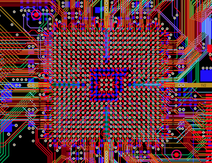
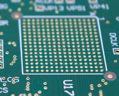
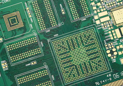
Microvias Structures of HDI PCB : |
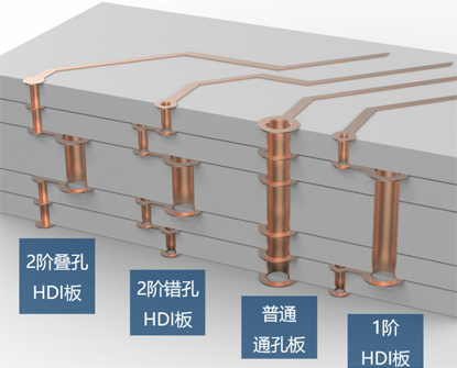
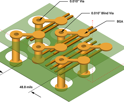
Microvias are small holes drilled into the layers of a High Density Interconnect (HDI) Printed Circuit Board (PCB) that enable interconnections between different layers. These microvias play a crucial role in achieving high circuit density and improved performance in modern electronic devices. There are several common microvia structures used in HDI PCBs: 1, Staggered Microvias: Staggered microvias are one of the most commonly used types of microvias in HDI PCBs. These microvias are drilled in a staggered pattern on different layers of the PCB, allowing for more efficient routing of signals and reducing the risk of signal interference. |
|
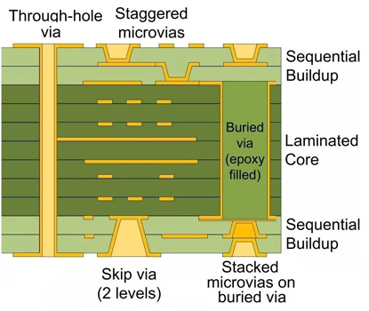 |
2, Stacked Microvias: Stacked microvias involve multiple microvias stacked on top of each other to create vertical interconnections between multiple layers of the PCB. This structure enables complex routing and high-density interconnects in a compact space. 3, Blind Microvias: Blind microvias connect an outer layer of the PCB to one or more inner layers without penetrating the entire board. These microvias are drilled from the surface of the board and are used to reduce signal propagation delays and improve signal integrity. 4, Buried Microvias: Buried microvias are completely contained within the inner layers of the PCB and do not extend to the outer layers. These microvias allow for high-density interconnects between inner layers while maintaining a smooth outer surface for component mounting. 5, Via-in-Pad Microvias: Via-in-pad microvias are microvias that are located directly under a component pad. By integrating the via within the pad, this structure reduces the footprint of the PCB and allows for closer placement of components, improving signal integrity and thermal performance. |
These various microvia structures in HDI PCBs enable designers to achieve higher circuit density, improved signal integrity, and greater design flexibility in compact electronic devices such as smartphones, tablets, wearables, and other high-performance electronics. |
|
Different Stack-Up of HDI PCB : |
HDI (High Density Interconnect) PCBs can have various stack-up configurations, each tailored to meet specific design requirements and performance criteria. The stack-up of an HDI PCB refers to the arrangement of different layers of conductive and insulating materials that make up the printed circuit board. Here are some common stack-up configurations for HDI PCBs: 1, 1+N+1 Stack-up: This configuration consists of a single core layer with additional build-up layers on one or both sides. The "N" represents the number of build-up layers. This stack-up is often used for relatively simple HDI designs and provides increased routing density compared to traditional PCBs. |
|
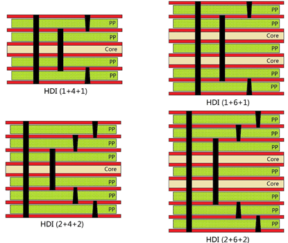 |
2, 2+N+2 Stack-up: In this configuration, there are two core layers with multiple build-up layers on both sides, providing even higher routing density and interconnect capability. The "N" denotes the number of build-up layers on each side of the core layers. 3, i+N+i (i≥3) Stack-up: contains 3 or more step "build-up" of high density interconnection layers. Blind vias on different layers can be laser drilled or stacked, Copper filled stacked microvia structures are commonly seen in demanding HDI designs. 4, Any-layer HDI Stack-up: This advanced stack-up allows for microvias to be placed on any layer of the PCB, enabling highly dense interconnections and intricate routing. It offers maximum flexibility in routing and interconnect options but requires specialized fabrication processes. Each of these stack-up configurations can be tailored further to accommodate specific design considerations such as impedance control, signal integrity, power distribution, thermal management, and component placement requirements. Designers carefully select the appropriate stack-up based on the complexity circuit,and electrical performance. |
By utilizing these various stack-up configurations, HDI PCBs can achieve higher circuit density, improved signal integrity, and enhanced functionality, making them ideal for applications requiring miniaturization and high-performance electronic capabilities. |
|
Any Layer Interconnection Technology of HDI PCB : |
● Any layer interconnection technology, also known as Any-Layer Via (ALV) technology, is an advanced interconnection technique used in HDI PCB design. It allows for the creation of highly dense interconnects that can span across any layer of the PCB, providing greater flexibility in layout and enabling more compact and efficient designs. It is mainly for high-level interconnection applications since any of the two layers in the PCB can be interconnected without any restriction. In other words, any-layer technology has higher flexibility in the layout, which saves the PCB space at least 30%. |
|
 |
● Unlike traditional PCBs, where vias are restricted to specific layers, ALV technology allows for the creation of vias that can penetrate through all layers of the PCB. This is achieved by using laser drilling to create microvias that are then filled with conductive material to create stacked microvia structures. ● One of the key advantages of any-layer interconnection technology is its ability to provide a reliable interconnect solution for highly complex large pin-count devices, such as CPU and GPU chips used in handheld and mobile devices. By allowing for greater routing density and reduced signal propagation delays, this technology can help improve the electrical characteristics of the PCB. ● However, the complexity of the ALV fabrication process means that it can be more expensive than conventional PCB technologies, and it requires specialized equipment and expertise. The ALV process involves multiple steps, including laser drilling, copper plating, inner-layer image transfer and press, and outer-layer imaging transfer, which must be carefully controlled to ensure high yields and consistent quality. |
● Any-layer interconnection technology is an advanced interconnect technique used in HDI PCBs, providing greater flexibility, improved routing density, and superior electrical performance. While it does come with higher costs and technical requirements, it offers significant benefits for applications requiring high-density interconnects and miniaturization. |
|
Advantages of High Density Interconnect PCB : |
HDI (High Density Interconnect) PCBs offer several advantages over traditional PCBs, making them a popular choice for modern electronic devices. Here are some of the key advantages of HDI PCBs: 1, Enhanced Functionality: HDI PCBs enable enhanced functionality by accommodating more components, features, and functionality in a smaller form factor. The increased routing density and interconnect capability of HDI PCBs make it possible to integrate more complex systems and functions on a single board. |
|
 |
2, Higher Circuit Density: HDI PCBs allow designers to achieve much higher circuit density than traditional PCBs. With advanced interconnection technologies like microvias, sequential lamination, and through-silicon vias, designers can create smaller and more complex circuitry in a compact space. 3, Improved Thermal Management: HDI PCBs enable better thermal management by providing more efficient heat dissipation paths and reducing thermal resistance. This helps prevent overheating and improves the reliability and lifespan of electronic devices. 4, Improved Signal Integrity: HDI PCBs provide better signal integrity due to their reduced signal propagation delay and lower electromagnetic interference (EMI). This is especially important for high-speed applications where timing and signal quality are critical. 5, Reduced Power Consumption: HDI PCBs can help reduce power consumption in electronic devices by minimizing the length of signal traces and reducing parasitic capacitance. This allows for more efficient use of power battery life in portable devices. |
6, Cost Savings: HDI PCBs can help reduce overall production costs by eliminating the need for additional boards, reducing assembly time, and minimizing material waste. While the initial cost of HDI PCBs may be higher than traditional PCBs, the improved functionality and performance can justify the investment in the long run. The advantages of HDI PCBs include higher circuit density, improved signal integrity, enhanced functionality, reduced power consumption, improved thermal management, and cost savings. These benefits make HDI PCBs an excellent choice for applications requiring miniaturization, high-density interconnects, and advanced functionality. |
|
Applications of HDI PCB : |
HDI (High Density Interconnect) PCBs have a wide range of applications across various industries. Here are some of the most common applications of HDI PCBs: 1, Consumer Electronics: HDI PCBs are commonly used in consumer electronics devices such as smartphones, tablets, laptops, and wearables. The small size and high-density interconnects of HDI PCBs make them ideal for miniaturized electronic devices where space is limited. |
|
 |
2, Automotive Electronics: Modern automotive electronics require high-performance and reliability. HDI PCBs can help meet these requirements by providing improved signal integrity, thermal management, and reduced power consumption. 3, Medical Devices: Medical devices such as implantable pacemakers, defibrillators, and neurostimulators require high-density interconnects and miniaturization. HDI PCBs can provide the necessary interconnect density while maintaining reliability and functionality. 4, Industrial Automation: Industrial automation systems require high-density interconnects and reliable performance in harsh environments. HDI PCBs can provide the necessary interconnect density and thermal management capabilities to meet these requirements. 5, Networking and Communications: Networking and communication devices require high-speed data transfer and low latency. HDI PCBs can provide the necessary signal integrity and routing density to support these requirements. |
6, Aerospace and Defense: Aerospace and defense applications require high-performance, reliability, and ruggedness. HDI PCBs can provide the necessary interconnect density while maintaining resistance to shock, vibration, and extreme temperatures. HDI PCBs are widely used in various applications that require miniaturization, high-density interconnects, advanced functionality, and improved performance. With their ability to provide higher circuit density, improved signal integrity, enhanced thermal management, and reduced power consumption, HDI PCBs are an essential component of modern electronic devices across multiple industries. |
|
Design Considerations of HDI PCB : |
Designing an HDI (High Density Interconnect) PCB requires careful consideration of several factors. Here are some of the key design considerations for HDI PCBs: 1, Layer Count: HDI PCBs typically have more layers than traditional PCBs. The layer count is determined by the number of signals, components, and functions that need to be integrated into the PCB. The layer count can impact the overall cost and performance of the PCB. 2, Impedance Control: Impedance control is critical in high-speed and high-frequency applications. The impedance of the traces must be carefully controlled to prevent signal degradation and crosstalk. This can be achieved through proper trace width, spacing, and routing techniques. |
|
 |
3, Signal Integrity: Signal integrity is essential in HDI PCBs to ensure reliable data transmission. Proper ground and power plane layout, via placement, and termination techniques must be considered to minimize signal loss and noise. 4, Via Management: HDI PCBs rely heavily on vias to create interconnections between layers. Via management is crucial to ensure proper signal routing and avoid signal interference. Proper via placement and sizing can help improve signal integrity and reduce EMI. 5, Component Placement: Component placement is critical in HDI PCBs due to the limited space available. Careful consideration must be given to component size, placement, and orientation to optimize the use of space and ensure proper functionality. 6, Thermal Management: Thermal management is important in HDI PCBs to prevent overheating and ensure reliability. Proper heat dissipation paths, thermal vias, and copper filling techniques can help manage heat in the PCB. |
7, Manufacturability: HDI PCBs are more complex to manufacture than traditional PCBs. The design must consider the fabrication process, such as laser drilling, plating, and lamination, to ensure a high yield rate and consistent quality. Designing HDI PCBs requires careful consideration of several factors, including layer count, impedance control, signal integrity, via management, component placement, thermal management, and manufacturability. By addressing these design considerations, designers can create high-quality HDI PCBs that meet the requirements of modern electronic devices. |
|
Manufacturing Challenges of High Density Interconnect PCB : |
Manufacturing HDI (High Density Interconnect) PCBs presents a unique set of challenges compared to traditional PCB manufacturing. Here are some of the key challenges faced in the manufacturing process of HDI PCBs: 1, Miniaturization: HDI PCBs are designed with smaller features, such as microvias and fine-pitch components, to achieve high circuit density. Miniaturization requires advanced manufacturing techniques, precise equipment, and strict process control to ensure accurate placement, routing, and via drilling. 2, Complex Layer Stacking: HDI PCBs often have multiple layers with intricate interconnections. Achieving precise layer stacking and alignment during lamination is crucial for maintaining signal integrity and preventing defects. This requires careful control of materials, temperature, pressure, and processing time during the lamination process. |
|
 |
3, Microvia Fabrication: Microvias are essential for achieving high-density interconnects in HDI PCBs. Manufacturing microvias involves laser drilling, plating, and filling processes. The challenges include maintaining uniform via dimensions, preventing debris or resin entrapment, and ensuring proper plating adhesion and conductivity. 4, Material Selection: HDI PCBs require specific materials that can meet the demands of miniaturization, thermal management, and signal integrity. Selecting suitable materials with appropriate dielectric properties, thermal conductivity, CTE (Coefficient of Thermal Expansion), and compatibility with manufacturing processes is crucial for reliable performance. 5, Registration and Alignment: Precise registration and alignment are critical when assembling HDI PCBs. Fine-pitch components, such as BGAs (Ball Grid Arrays) and CSPs (Chip Scale Packages), require accurate placement to ensure proper solder joint formation and electrical connections. Misalignment or registration errors can lead to solder defects, open circuits, or short circuits. |
6, Quality Control and Inspection: HDI PCB manufacturing requires stringent quality control and inspection processes. The complexity and miniaturization of HDI PCBs make it challenging to detect defects, such as microvia voids, plating thickness variations, or misaligned vias. Advanced inspection techniques, such as automated optical inspection (AOI), X-ray inspection, and electrical testing, are necessary to ensure the quality and reliability of HDI PCBs. 7, Cost: HDI PCBs typically have higher manufacturing costs compared to traditional PCBs due to the complexity of processes involved, specialized equipment requirements, and the use of advanced materials. Ensuring a balance between cost-effectiveness and meeting design requirements is a challenge in HDI PCB manufacturing. Manufacturing HDI PCBs involves overcoming challenges related to miniaturization, complex layer stacking, microvia fabrication, material selection, registration and alignment, quality control and inspection, and cost. Addressing these challenges requires advanced equipment, precise process control, and expertise in HDI PCB manufacturing techniques. |
|
Why Choose PANDA PCB For HDI PCB ? |
● Unmatched Expertise: With 20 years of experience in the industry, we have mastered the art of manufacturing HDI PCBs. Our team of skilled professionals ensures that every PCB we produce meets the highest standards of quality and precision. |
|
 |
● Cutting-Edge Technology: We believe in staying ahead of the curve. That's why we invest in state-of-the-art technology and equipment to manufacture HDI PCBs with the latest advancements. You can trust us to deliver PCBs that are at the forefront of technological innovation. ● Customization at its Best: At Panda PCB, we understand that every project is unique. That's why we offer customizable solutions to meet your specific requirements. Whether it's complex layer stacking or tight design constraints, we have the expertise to deliver tailor-made HDI PCBs. ● Reliable and Timely Delivery: We value your time and understand the importance of meeting deadlines. Our streamlined production process ensures that your HDI PCBs are manufactured and delivered to you on time, every time. Trust us to be your reliable partner in PCB manufacturing. |
● Exceptional Customer Support: We believe in building long-term relationships with our clients. Our dedicated customer support team is always ready to assist you at every step of the process. From initial consultation to after-sales support, we are committed to providing you with the best service possible. Make the smart choice for your HDI PCB needs. Choose Panda PCB and experience excellence in every aspect. Contact us today to discuss your requirements and let us take your projects to new heights! |
|
Process Capabilities of HDI PCB: |
Design Rules of HDI PCB : |
||||||||||||||||||||||||||||||||||||||||||||||||||||||||||||||||||||||||||||||
|
|