Thick Film Hybrid Circuit
What is Thick Film Hybrid Circuit ?
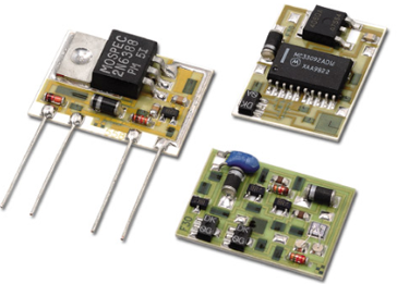
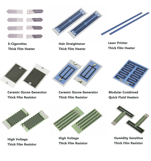
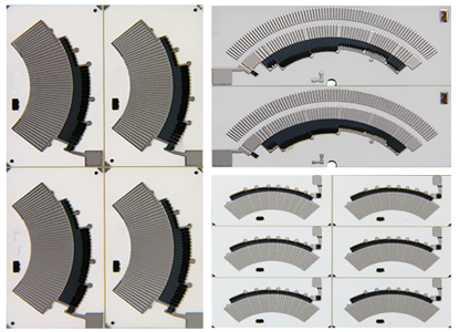
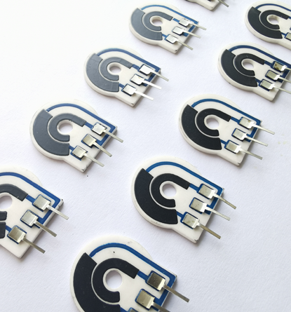
Thick Film Hybrid Circuit also calls Thick Film Resistor Hybrid Circuit is the physical realization of an electronic circuit from two or more discrete circuit elements, like integrated circuits, transistors, diodes, resistors, capacitors, transformers and conductors. These are usually mounted on an insulating ceramic substrate to produce circuit functions similar to but with advantages over monolithic integrated circuits. Thick Film Hybrid Circuits are made with the substrate depositions designed and fabricated by screen printing; and then firing of layers of highly viscous pastes composed of noble metal powders, vitreous binders etc. Thick Film Hybrid Circuit Technology is ideally suited when quick turnaround is required for complex, high density multi-layer, low cost, high volume applications. It is also extremely effective for development work, quite often surpassing PCB turnaround. The ability to print resistors, capacitors, and inductors on ceramic based substrates allows for increased package density and reliability. |
 |
||||
|
|||||
|
Basic Parameter of Thick Film Hybrid Circuit |
1> Ceramic Substrate can be 96% or 98% Alumina (Al2O3) or Beryllium Oxide (BeO), thickness range: 0.25, 0.38, 0.50mm, 0.635mm (default thickness), 0.76mm, 1.0mm. Thicker thickness such as 1.6mm or 2.0mm can be customized too. 2> Conductor layer materail is silver palladium, gold palladium, or Mo/Mu+Ni (for Ozone); 3> Thickness of conductor >= 10 miron (um), and Max can be 20 micron (0.02mm) 4> Min trace width and space for volume production:0.30mm & 0.30mm, 0.20mm/0.20mm is also okay but cost will be higher, and 0.15mm/0.20mm only available for prototype. 5> Tolerance for final trace layout will be +/-5% 6> Both gold and silver palladium is workable for gold-wire bonding, but customer need to mention that so that we will use special silver palladium which is suitable for that artwork. 7> More different resistor value on the same board, more expensive board will be 8> Normally layers are 1L and 2L (with plated through hole (PTH), and plated material is the same like the one used for conductor), and maximum layers can be 10 layers 9> Soldermask is also available upon request, working temperature >500 C, and color is semi-transparent. 10> Lead out: SIP and DIP, Pitch2.54mm and1.78mm 11> Die assembly and AI wedge bonding |
The most representative applications of Thick Film Carbon Hybrid Circuit are: |
|
Application in Industrial, Communication and National Defense: |
|
 |
 |
| Engineering Specifications: | |
(1).Printing Accuracy: ±2 mil |


