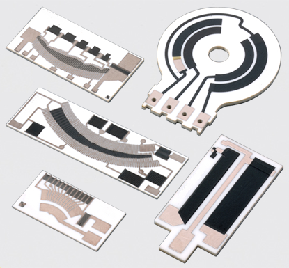
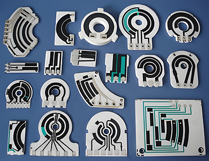
Thick Film Ceramic PCB
Thick Film Ceramic PCBs are high-performance printed circuit boards made with ceramic as the base substrate, offering excellent thermal conductivity, high mechanical strength, and outstanding integration and customization capabilities, utilizing thick film hybrid circuit technology to print and cure conductive, resistive, and insulating materials layer by layer, followed by high-temperature sintering and laser trimming processes, ultimately forming special circuit boards with high-precision resistance, capacitance, or sensor functions, which are widely used in advanced electronic systems and industries with strict requirements. Thick Film Ceramic PCBs are built with ceramic substrates like alumina (aluminum oxide) or aluminum nitride, which offer superior thermal conductivity, mechanical strength, and chemical resistance compared to the traditional fiberglass epoxy (FR4) substrate found in standard PCBs. These ceramic materials make the PCBs highly suitable for applications in environments that demand high thermal management and resistance to harsh chemicals, mechanical stresses, and extreme temperatures. Thick Film Ceramic PCBs are specifically designed for applications where conventional PCB technologies cannot meet the required performance standards. In these applications, common conductor pastes, such as gold paste, silver paste, silver-platinum paste, and palladium alloys, are used to form the electrical interconnections. These thick-film materials are sintered at temperatures ranging from 400 to 850°C, resulting in highly durable, stable, and reliable interconnections that can withstand rigorous operating conditions over long periods. Main Features of Thick Film Ceramic PCB : |
 |
|
 |
1, Material: Thick film ceramic PCBs are made of a specialized ceramic material that provides excellent thermal conductivity, high insulation resistance, and superior mechanical strength. This makes them suitable for applications requiring efficient heat dissipation and robustness. 2, High Power Handling: The thick film ceramic material used in these PCBs allows for efficient power handling capabilities, making them ideal for high-power applications such as power electronics, LED lighting, and automotive electronics. 3, Compact Design: Thick film ceramic PCBs can be manufactured with thin layers, enabling the creation of compact and lightweight circuit designs. This is particularly beneficial in space-constrained applications where size and weight reduction are crucial. |
|
4, Excellent Thermal Management: The ceramic material used in these PCBs offers exceptional thermal conductivity, allowing for efficient dissipation of heat generated by components. This feature helps in maintaining optimal operating temperatures and extends the lifespan of electronic devices. 5, Stability and Reliability: Thick film ceramic PCBs exhibit excellent stability and reliability due to their high insulation resistance, low coefficient of thermal expansion, and resistance to moisture, chemicals, and environmental factors. This makes them suitable for demanding applications that require long-term performance and durability. 6, Design Flexibility: Thick film ceramic PCBs can be customized to meet specific design requirements. They support a wide range of circuit designs, including both surface mount technology (SMT) and through-hole components. Additionally, they can be fabricated with various conductor materials, such as gold, silver, or platinum. 7, Compatibility: Thick film ceramic PCBs are compatible with standard manufacturing processes, making them easy to integrate into existing production lines. They can also be seamlessly combined with other PCB technologies, such as multilayer construction or embedded passive components, to enhance functionality. Thick Film Ceramic PCBs offer excellent thermal management, high power handling capabilities, compact designs, and superior reliability. These features make them suitable for a wide range of applications, including power electronics, LED lighting, aerospace, automotive, and medical devices. Please check Thick Film Resistor PCB for more informations. |
||
Design Guidelines of Thick Film Ceramic PCB : |
 |
The design guidelines for Thick Film Ceramic PCBs encompass several key considerations to ensure optimal performance and reliability. Here are some important design guidelines for thick film ceramic PCBs: 1, Thermal Management: Consider the thermal conductivity of the ceramic material and plan for effective heat dissipation from high-power components. 2, Component Placement: Strategically place components to optimize circuit performance and heat dissipation, considering the thermal characteristics of the ceramic substrate. 3, Trace Width and Spacing: Adhere to appropriate trace width and spacing requirements to maintain electrical integrity and prevent signal interference. 4, Material Selection: Choose compatible materials for conductive and resistive layers to ensure proper adhesion and performance under varying environmental conditions. 5, Environmental Considerations: Account for the operating environment to select materials that can withstand temperature extremes, humidity, and chemical exposure. |
6, Rounded Corners: Implement rounded corners in the design to minimize stress concentration and enhance the mechanical reliability of the PCB. 7, Solder Mask and Surface Finish: Specify the appropriate solder mask and surface finish to safeguard against oxidation and facilitate soldering processes. 8, Test Points and Probing: Incorporate designated test points for troubleshooting and probing during the testing and assembly stages. 9, Design for Manufacturing (DFM): Optimize the design for manufacturability by considering standard fabrication processes and minimizing complexities that could impede production efficiency. 10, Reliability Considerations: Design with reliability in mind, ensuring robustness against mechanical stress, thermal cycling, and long-term operation. By adhering to these design guidelines, engineers can harness the advantages of Thick Film Ceramic PCBs and create robust, high-performance electronic systems tailored to specific application requirements. |
|
Engineering Parameters of Thick Film Ceramic PCB : |
 |
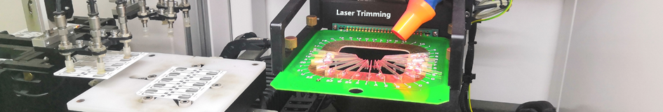
1, Ceramic Substrates: The ceramic substrates can be made of 96% or 98% Alumina (Al2O3) or Beryllium Oxide (BeO). The thickness ranges from 0.25mm, 0.38mm, 0.50mm, 0.635mm, 0.76mm, 1.0mm, 1.2mm, 1.6mm to 2.0mm. Customizable thickness options are also available. 2, Conductive Paste Materials: Various conductive paste materials can be used, such as silver paste, silver-palladium, gold-palladium, or Mo/Mu+Ni (for Ozone applications). 3, Conductors Thickness: The thickness of the conductors is typically 12um+/-5um, with a maximum thickness of 20um+/-5um. 4, Resistor Value Tolerance: The resistor value tolerance is typically set at +/-10% (customizable). Linearity can be achieved at less than 1%, 0.5%, or even 0.2% through laser trimming. The durability of carbon ink (life time) is usually between 2-5 million cycles. 5, Minimum Trace Width and Space: For volume production, the minimum trace width and space are typically 0.30mm/0.30mm. A tighter option of 0.20mm/0.20mm is also feasible but comes at a higher cost. And 0.15mm/0.20mm is only available for prototype. |
6, Compatibility with Gold and Silver Palladium: Both gold and silver palladium can be used for gold-wire bonding. If gold paste is required, please inform us so that we can utilize a special gold palladium paste suitable for this purpose. 7, Multiple Resistor Values: Incorporating different resistor values on the same board will increase the overall cost of the PCB. |
|
 |
8, Cost Considerations: Gold-palladium is significantly more expensive than silver, with a cost that can be 2-5 times higher. 9, Layer Options: Typically, thick film ceramic PCBs can have 1 layer (single-sided) or 2 layers (with Via metallization and plated through holes). The plating material used for conductors is the same throughout the PCB. 10, Linearity: For most thick film ceramic sensor products, the resistor strip usually needs to achieve a function of controlling signal transmission to be linearity or synchronous. For example, our conventional linearity can be <1.0%. If customers require higher accuracy, laser trimming can be used to achieve 0.25%. 11, Durability (Lifetime): For ceramic sensors designed as a linear potentiometers, There will be a contact wiper slides on the surface of the carbon film to change its resistance value. However, the wiper can also cause wear on the resistor surface during sliding, so customers have strict requirements for the durability of carbon film. Our standard carbon film has a durability of up to 5 million cycles. If higher is required, a polishing process can be used to achieve over 10 million cycles, but cost higher. |
Typical Applications of Thick Film Ceramic PCB : |
Thick Film Ceramic PCBs (Printed Circuit Boards) are widely used in various electronic applications due to their excellent thermal conductivity, high temperature resistance, and reliability. Some typical applications of thick film ceramic PCBs include: 1, Power Electronics: Thick film ceramic PCBs are commonly used in power electronic devices such as power supplies, motor drives, and inverters due to their high thermal conductivity and ability to dissipate heat effectively. 2, LED Lighting: Thick film ceramic PCBs are used in LED lighting fixtures where high thermal performance is essential for maintaining the longevity and efficiency of the LEDs. |
 |
3, Automotive Electronics: In automotive applications, thick film ceramic PCBs are utilized in engine control units, transmission control modules, fuel level sensor, throttle position sensor and other systems that require high temperature resistance and reliability. 4, Renewable Energy Systems: Thick film ceramic PCBs are used in renewable energy systems such as solar inverters and wind power electronics where efficient heat dissipation and reliability are crucial. |
|
5, Aerospace and Defense: Due to their ability to withstand extreme temperatures and harsh environments, thick film ceramic PCBs are used in aerospace and defense applications for avionics, radar systems, and communication equipment. 6, Medical Devices: Thick film ceramic PCBs are employed in medical devices such as patient monitoring systems, diagnostic equipment, and medical imaging devices where reliability and performance under varying conditions are critical. 8, Industrial Controls: Many industrial control systems benefit from the use of thick film ceramic PCBs due to their reliability, high temperature tolerance, and resistance to harsh industrial environments. |
 |
9, Telecommunications: In telecommunications infrastructure, thick film ceramic PCBs find application in base stations, transceivers, and network equipment due to their thermal properties and reliability. These are just a few examples of the typical applications of thick film ceramic PCBs, showcasing their versatility and suitability for demanding electronic systems across various industries. |
|
Advantages of Thick Film Ceramic PCB : |
 |
Thick Film Ceramic PCBs offer several advantages over other types of printed circuit boards, making them a preferred choice for various electronic applications. Some of the key advantages include: 1, High Thermal Conductivity: Thick film ceramic PCBs exhibit excellent thermal conductivity, allowing them to efficiently dissipate heat generated by electronic components. This property is particularly beneficial in high-power applications and in electronic devices that require effective heat management. 2, High Temperature Resistance: Ceramic materials have inherent resistance to high temperatures, and thick film ceramic PCBs can withstand elevated operating temperatures without degrading or compromising performance. This makes them suitable for use in harsh and demanding environments where temperature fluctuations are common. 3, Long Term Reliability: Most commercially packaged semiconductors will have a life span measured in years, while ceramic PCBs have a life span measured in decades. |
4, Reliability and Durability: The robust nature of ceramic materials contributes to the overall reliability and durability of Thick Film Ceramic PCBs. They are less prone to mechanical and thermal stress, which enhances the longevity of the electronic systems in which they are used. 5, Chemical and Corrosion Resistance: Ceramic materials are highly resistant to chemical exposure and corrosion, making Thick Film Ceramic PCBs suitable for applications where contact with harsh chemicals or corrosive substances is a concern. |
|
 |
6, Low Failure Rate: Aside from long term reliability, Thick film ceramic PCBs also exhibit a lower mean time between failure rate when exposed to environmental stresses such as high temperature, mechanical vibration or other harsh conditions. 7, Miniaturization: The ability to create thin and compact PCBs using thick film ceramic technology contributes to the miniaturization of electronic devices, which is particularly important in industries such as consumer electronics and portable devices. 8, Hermetic Sealing: Thick film ceramic PCBs can be hermetically sealed, providing protection against moisture, dust, and other environmental contaminants. This feature is advantageous in applications where the integrity of the electronic system needs to be preserved. 9, Design Flexibility: Thick film ceramic PCBs can be designed with a high degree of flexibility in terms of circuit layout, component placement, and integration of passive components. This design flexibility allows for optimized performance and efficient use of space within electronic devices. |
10, Compatibility with High-Frequency Signals: Ceramic materials exhibit good electrical properties, making Thick Film Ceramic PCBs suitable for high-frequency and RF (radio frequency) applications where signal integrity and minimal signal loss are critical. 11, Multi-Layers: Thick Film Ceramic PCBs can be designed to be a multi-layer hybrid circuit with complicated task. With the toughness of its material, another layer can be added easily and still keep the other components safe. Ceramic hybrid circuit is excellent for heavy-duty applications. These advantages collectively position Thick Film Ceramic Sensors as a desirable choice for electronic designers and manufacturers seeking reliable, high-performance solutions for a wide range of applications. |
|
Applications In Automotive Industry of Thick Film Ceramic PCB : |
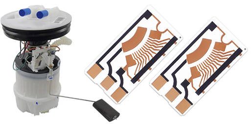
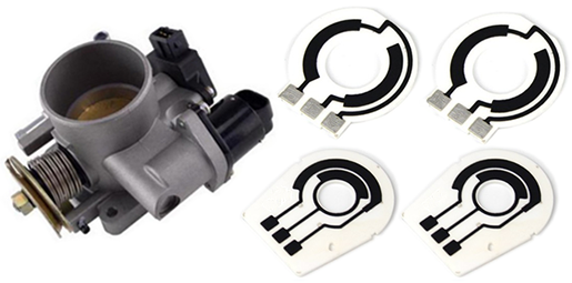
Thick Film Ceramic PCB (Thick Film Ceramic Printed Circuit Board) technology has found numerous applications in the automotive industry, particularly in the development of various sensors. Two representative examples are fuel level sensors and throttle position sensors. |
|
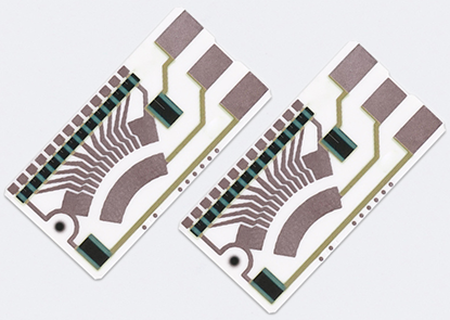 |
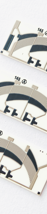
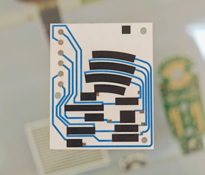
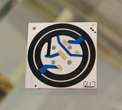
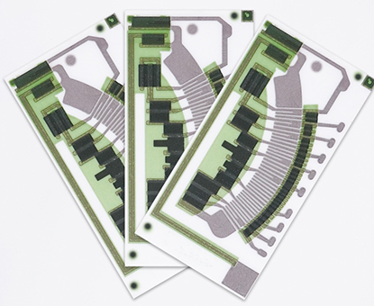
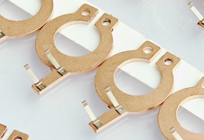
1, Fuel Level Sensor Ceramic PCB: Thick Film Ceramic PCBs are used in fuel level sensors to accurately measure the amount of fuel present in a vehicle's fuel tank. These sensors typically consist of a ceramic substrate that acts as a base for the thick film circuitry. The conductive, resistive, and dielectric materials are printed onto the ceramic substrate using a screen printing process. These materials form the sensing elements and provide the necessary electrical connections. The thick film ceramic PCBs in fuel level sensors offer several advantages: ● Resistance to temperature variations and chemical exposure, ensuring reliable performance in harsh automotive environments. ● High precision and accuracy in fuel level measurement, enabling accurate reading of remaining fuel quantity. ● Compact size and lightweight design, allowing easy integration into the fuel system. |
● Materials: The term "Ceramic" in the context of a PCB refers to the substrate material used for the board, which is ceramic. Ceramic substrates offer excellent thermal and electrical properties, making them suitable for high-temperature and high-frequency applications. ● Construction: The sensor typically consists of a resistive element that changes resistance as the fuel level changes. This change is detected by the PCB, which converts the resistance variation into an electrical signal. ● Integration: The Ceramic PCB is designed to integrate with the sensor's electronic components, providing a stable and reliable platform for signal processing and transmission to the vehicle's control unit. |
|
 |
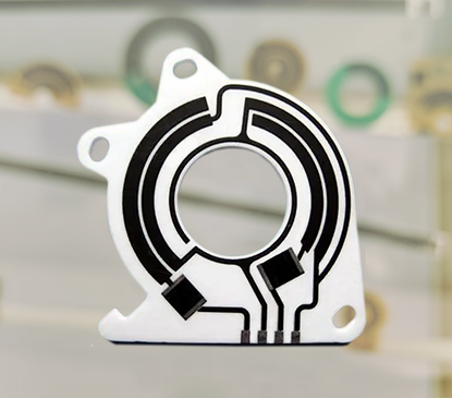
2, Throttle Position Sensor Ceramic PCB: Thick Film Ceramic PCBs are also employed in throttle position sensors, which monitor the position of the throttle valve in an engine. These sensors help regulate the airflow, fuel injection, and overall engine performance. The thick film ceramic PCBs used in throttle position sensors facilitate the construction of robust and efficient sensors. Key benefits of using thick film ceramic PCBs in throttle position sensors include: ● Excellent thermal stability, ensuring consistent performance across a wide range of temperatures. ●High mechanical strength, allowing the sensor to withstand vibrations and shocks associated with automotive applications. ● Compatibility with high-power circuits, enabling accurate measurement and transmission of throttle position data. |
● Function: Throttle Position Sensor (TPS) Ceramic PCB is used to detect the position of the throttle in a vehicle's engine. This information is crucial for the engine control unit (ECU) to manage the air-fuel mixture and the amount of fuel to be injected into the engine for optimal performance and fuel efficiency. ● Operation: The TPS usually has a variable resistor or a potentiometer whose resistance changes as the throttle is opened or closed. The Ceramic PCB is integral in translating these mechanical movements into electrical signals. ● Technology: Modern TPS Ceramic PCBs may also incorporate microcontrollers or integrated circuits to provide more accurate and complex signal processing, allowing for better engine management. ● Compatibility: These Ceramic PCBs are designed to be compatible with various vehicle makes and models, ensuring they can interface with different ECUs and throttle body designs. Thick Film Ceramic PCBs play a crucial role in the automotive field, particularly in the development of fuel level sensors and throttle position sensors. They offer durability, accuracy, and reliability required for critical automotive applications. |
|
Why Deed to Customize Thick Film Ceramic PCB ? |
1, Specialized Applications: Different industries and applications have unique requirements. Custom Thick Film Ceramic PCBs can be tailored to meet these specific needs, ensuring optimal performance in environments such as aerospace, automotive electronics, medical, or high-temperature industrial settings. 2, Improved Performance: Customization allows for the design and integration of components that can enhance the performance of the PCB. This can include the use of specialized materials, unique circuit layouts, special tolerance, and advanced thermal management solutions. |
|
 |
3, Reliability: Thick film ceramic PCBs are known for their reliability and durability. Customization can further improve this by incorporating design features that mitigate risks of failure, such as redundant circuits or enhanced soldering techniques. 4, Miniaturization: As technology advances, there is a constant demand for smaller and more compact devices. Custom thick film ceramic PCBs can be designed to occupy minimal space while still providing the necessary functionality. 5, Cost Efficiency: While there may be an initial investment in customizing a thick film ceramic PCB, the long-term benefits can include cost savings. Custom designs can eliminate unnecessary components, reduce waste, and streamline manufacturing processes. 6, Innovative Design: Customization enables engineers to push the boundaries of design, incorporating the latest technologies and materials into their PCBs. This can lead to innovative products that stand out in the market. |
7, Flexibility: Custom Thick Film Ceramic PCBs offer flexibility in terms of design and material selection. This allows manufacturers to adapt quickly to changing market demands or to incorporate new technologies as they become available. 8, Long-term Partnerships: Working with a PCB manufacturer to create a customized solution can foster a strong, long-term partnership. This can lead to ongoing collaboration and support, ensuring that future projects are also successful. 9, Brand Differentiation: Custom Thick Film Ceramic PCB can help differentiate a product in a crowded market. It shows that a company is willing to invest in unique solutions to meet their customers' needs. Custom Thick Film Ceramic PCB is a strategic decision that can lead to better product performance, increased reliability, and a competitive edge in the marketplace. It is an investment that pays off by providing a tailored solution that meets the exact specifications and requirements of the application at hand. |
|
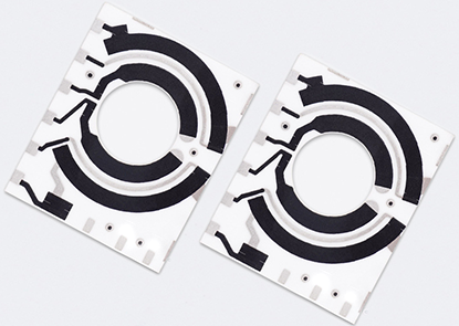
Multi-Wire Wipers Used For Thick Film Ceramic PCB : |
 |
1, For ceramic sensors designed as a linear or rotary potentiometers, There will be a contact wiper slides on the surface of the carbon film to change its resistance value. The wiper is a key element designed to transmit voltage and signals. It performs a linear or rotational sliding on the surface of resistive materials (thick film resistor) to change resistance values and serve as a contacter of voltage divider. 2, Wiper design is extremely critical for the efficiency and life of the sensor assembly, When designing the wiper, it is very important to consider contact resistance, working-hight (load), repeatability, hysteresis, the resistive material used, and in particular, the wiper material itself, its shape and the wiper pressure. 3, We also provided custom Multi-Wire Wipers for customer if needs, we can manufacture the wipers according to customer's design requirements or specification, For more information about wipers, Please refer to Multi-Contact Wipers. |
Capabilities of Thick Film Ceramic PCB Are As Follows : |
1, Engineering Specification of Thick Film Ceramic PCB :
Items : |
Typical Values |
Advanced Capabilities |
1, Substrates : |
FR4, Ceramic ( AI203, ALN, BeO, ZrO2), Polyimide (Flexible PI), Stainless Steel (SUS304), Mica |
FR4, Ceramic ( AI203, ALN, BeO, ZrO2), Polyimide (Flexible PI), Stainless Steel (SUS304), Mica |
2, Conductor (Paste) Materials : |
Copper, Silver , Gold , Silver-Palladium, Palladium-Gold, Platinum-Silver, Platinum-Gold |
Copper, Silver , Gold , Silver-Palladium, Palladium-Gold, Platinum-Silver, Platinum-Gold |
3, Thick Film Carbon Thickness (Height) : |
15um +/-5 um |
30um +/-5 um |
4, Conductor Thickness (Height) : |
12um+/-5um |
20um+/-5um |
5, Min Width of Thick Film Line : |
0.30 mm +/-0.05 mm |
0.20 mm +/-0.05 mm |
6, Min Space of Thick Film Line : |
0.30 mm +/-0.05 mm |
0.20 mm +/-0.05 mm |
7, Min Overlap (Carbon to Conductor) : |
No less than 0.25mm |
0.20mm (Minimum) |
8, Sheet Resistivity (ohms/square): |
Printed resistors in milli ohm to mega ohm range (Customizable) with tolerances of 1-10% are fabricated and protected with overglaze materials. |
Printed resistors in milli ohm to mega ohm range (Customizable) with tolerances of 0.5-10% are fabricated and protected with overglaze materials. |
9, Resistor Value Tolerance (ohms) : |
+/-10.0% (Standard) (Customizable) |
+/-0.5% (Laser trimming) |
10, Linearity : |
+/-1.0% (Standard) (Customizable) |
+/-0.2 ~ +/-0.5% (Laser trimming) |
11, Synchronism of Double Channels : |
+/-2.0% (Standard) (Customizable) (Potentiometers) |
+/-1.0% (Laser trimming) (Potentiometers) |
12, Durability of Carbon Ink (Life time) : |
0.5 Million (Min), 2.0 Million (Standard) |
5.0-10.0 Million (Max) with Surface Polishing |
13, Working Temperature : |
- 40ºC /+150ºC |
- 40ºC /+180ºC |
2, Optional Processes of Thick Film Ceramic PCB :
Metalization Types : |
Thick Film Substrates (Screen-Printed) |
Thin Film Substrates (Photo-Imaged) |
|||
Process Types : |
TFM Capabilities |
HTCC / LTCC Capabilities |
DBC Capabilities |
DPC Capabilities |
AMB Capabilities |
Layer Counts : |
1, 2, 3, 4, 5, 6 Layers |
1, 2, 4, 6, 8, 10, 12 Layers |
1, 2 Layers |
1, 2 Layers |
1, 2 Layers |
Max Board Dimension : |
200*230mm |
200*200mm |
138*178mm |
138*190mm |
114*114mm |
Min Board Thickness : |
0.25mm |
0.25mm |
0.30mm~0.40mm |
0.25mm |
0.25mm |
Max Board Thickness : |
2.2mm |
2.0mm |
1L: 1.6mm; 2L 2.0mm |
2.0mm |
1.8mm |
Conductor Thickness : |
10um - 20um |
5um - 1500um |
1oz - 9oz |
1um - 1000um |
1oz- 22oz |
Min Line Width/Space : |
8/8mil (0.20/0.20mm) |
6/6mil (0.15/0.15mm) |
10/10mil (0.25/0.25mm) |
6/6mil (0.15/0.15mm) |
12/12mil (0.30/0.30mm) |
Substrates Types : |
AI203, ALN, BeO, ZrO2 |
AI203, ALN, BeO, ZrO2 |
Al2O3, AlN, ZrO2, PbO, SiO2, ZTA, Si3N4, SiC, Sapphire, Polycrystalline Silicon, Piezoelectric Ceramics |
Al2O3, AlN, ZrO2, PbO, SiO2, ZTA, Si3N4, SiC, Sapphire, Polycrystalline Silicon, Piezoelectric Ceramics |
AI203, ALN, BeO, ZrO2, Si3N4 |
Min Hole Diameter : |
4mil (0.15mm) |
4mil (0.15mm) |
4mil (0.1mm) |
4mil (0.1mm) |
4mil (0.1mm) |
Outline Tolerance : |
Laser: +/-0.05mm; Die Punch: +/-0.10mm |
Laser: +/-0.05mm; Die Punch: +/-0.10mm |
Laser: +/-0.05mm; Die Punch: +/-0.10mm |
Laser: +/-0.05mm; Die Punch: +/-0.10mm |
Laser: +/-0.05mm; Die Punch: +/-0.10mm |
Substrate Thickness : |
0.25, 0.38, 0.50, 0.635, 0.80,1.0, 1.25, 1.5, 2.0mm, Customizable |
0.25, 0.38, 0.50, 0.635, 0.80,1.0, 1.25, 1.5, 2.0mm, Customizable |
0.25, 0.38, 0.50, 0.635, 0.80,1.0, 1.25, 1.5, 2.0mm, Customizable |
0.25, 0.38, 0.50, 0.635, 0.80,1.0, 1.25, 1.5, 2.0mm, Customizable |
0.25, 0.38, 0.50, 0.635, 0.80,1.0, 1.25, 1.5, 2.0mm, Customizable |
Thickness Tolerance : |
0.25-0.38: +/-0.03mm; 0.50-2.00: +/-0.05mm |
0.25-0.38: +/-0.03mm; 0.50-2.00: +/-0.05mm |
0.25-0.38: +/-0.03mm; 0.50-2.00: +/-0.05mm |
0.25-0.38: +/-0.03mm; 0.50-2.00: +/-0.05mm |
0.25-0.38: +/-0.03mm; 0.50-2.00: +/-0.05mm |
Surface Treatment : |
Ag, Au, AgPd, AuPd |
Ag, Au, AgPd, AuPd, Mn/Ni |
OSP/Ni Plating, ENIG |
OSP/ENIG/ENEPIG |
OSP/ENIG/ENEPIG |
Min Solder PAD Dia : |
10mil (0.25mm) |
10mil (0.25mm) |
8mil (0.20mm) |
6mil (0.15mm) |
8mil (0.20mm) |
3, Optional Substrates of Thick Film Ceramic PCB :
Substrates : |
Alumina (Al2O3) |
Aluminum Nitride (AlN) |
Beryllium Oxide (BeO) |
Zirconium Dioxide (ZrO2) |
Max Application Temperature : |
662 - 1832 |
1832 |
2300 |
2432 |
Max Power Density (W/in²): |
75 |
1010 |
250 |
300 |
Max Ramp Up Speed (°F/sec): |
122 |
572 |
400 |
350 |
Thermal Conductivity (W/mK): |
20-35 |
180-220 |
200-300 |
2.0-5.0 |
Density (g/cm³): |
3.75 |
3.26 |
2.8 |
5.9 |
Dielectric Loss: |
0.0001 - 0.001 |
0.0001 - 0.0005 |
0.0001 - 0.0002 |
0.0005 - 0.001 |
Dielectric Constant: |
9.4 - 10.2 |
8.5 - 9.0 |
6.0 - 7.0 |
25 - 30 |
CTE, ppm/ºC: |
6.0 - 8.0 |
4.0 - 5.0 |
7.0 - 9.0 |
10.0 - 11.0 |
Substrate Thickness (mm): |
0.25 - 2.0 |
0.25 - 2.0 |
0.25 - 2.0 |
0.25 - 2.0 |
Typical Max. Dimension (inch): |
6 x 12 |
5 x 11 |
6 x 6 |
4 x 4 |
Theoretical Total Wattage (W): |
5400 |
55000 |
15000 |
20000 |
4, Conductive Paste of Thick Film Ceramic PCB :
Paste ( Materials) : |
Conductor Width/Space |
Soldering / Bonding |
Gold : |
8/8mil (0.20/0.20mm) |
Gold is a good conductor material and allows thermo-compression gold wire bonding and eutectic die attachment. It is, of course, costly and has poor solderability. |
Silver : |
8/8mil (0.20/0.20mm) |
Soldering & Silver is lower in cost, and solderable, but is not leach-resistant with tin/lead solders.More seriously, silver atoms migrate under the influence of DC electric fields, both causing short-circuits and reacting with many of the resistor paste formulations. |
Platinum-Silver : |
6/6mil (0.15/0.15mm) |
Soldering & Surface Mount, Palladium and platinum alloyed to the gold and silver produce good conductor pastes,with good adhesion to the substrate, good solderability, and moderately good wire bonding characteristics. Copper and nickel are examples of materials that have been proposed for paste systems as substitutes for noble metals. |
Palladium-Silver : |
8/8mil (0.20/0.20mm) |
Soldering & Surface Mount ,Solderable, Wire bondable, (good aged adhesion general purpose), Silver-palladium conductor inks are the most commonly used materials, with both price and performance (primarily resistance to solder) increasing with palladium content. |
Platinum-Gold : |
6/6mil (0.15/0.15mm) |
Soldering & Au or Al Wire Bonding, Solderable (excellent aged adhesion with no migration). |
Palladium-Gold : |
8/8mil (0.20/0.20mm) |
Soldering & Au or Al Wire Bonding, Wire bondable. |
5, Resistive Paste of Thick Film Ceramic PCB :
Performances : |
Common Values/Range |
Description |
Resistance Value : |
1Ω to several MΩ |
The resistance value depends on the type and ratio of carbon black, typically ranging from 1Ω to Mega ohm. |
Resistance Tolerance : |
±1% to ±10% |
High-precision resistors can achieve ±0.1% tolerance used laser trimming process. |
Temperature Coefficient (TCR) : |
±50ppm/°C to ±200ppm/°C |
High-quality resistive paste should have a low TCR, preferably below ±100ppm/°C. |
Stability : |
≤1% |
Resistors must undergo high-temperature aging and humidity tests to ensure stability. |
Sintering Temperature : |
850°C to 950°C |
The sintering temperature for carbon paste depends on material properties, typically in this range. |
Conductivity : |
10⁶ S/m to 10⁸ S/m |
Conductivity depends on the type and ratio of carbon black, affecting resistance precision and stability. |
Surface Smoothness : |
Ra≤ 1 μm |
The surface must be free of cracks, bubbles, and non-uniform layers to ensure good mechanical and electrical properties. |
Insulation Resistance : |
≥10⁹ Ω |
Carbon paste should have good insulation properties to avoid leakage or short circuits. |
Mechanical Strength : |
≥100 MPa |
The resistive layer must have good compressive and bending strength to ensure the reliability of the resistor. |
Volatility : |
Solvent residue ≤ 1% |
High volatility solvents help with even coating and drying, but excessive volatility may affect electrical performance. |
Oxidation Resistance : |
>1000 hours |
High-quality carbon paste should have strong oxidation resistance to extend the service life. |
Humidity Resistance : |
≥1000 hours |
Resistors should be able to withstand high-humidity conditions to ensure long-term stable performance, no significant changes. |
6, Dielectric Paste of Thick Film Ceramic PCB :
1, High Dielectric Constant (Dk): This parameter determines the ability of the material to store electrical energy when exposed to an electric field. It's an important factor in determining the impedance and signal propagation characteristics of the PCB. 2, High Dielectric Loss (Df): Also known as dissipation factor, this parameter measures the amount of energy lost as heat for a given unit of energy stored in the dielectric material. It's an important consideration for high-frequency applications. 3, High Thermal Conductivity: This parameter indicates the material's ability to conduct heat. In thick film ceramic PCBs, good thermal conductivity helps in efficient heat dissipation, which is crucial for power applications. 4, High Adhesion Strength: The paste's adhesion strength to the substrate is essential for ensuring good performance and reliability of the PCB. 5, Low Coefficient of Thermal Expansion (CTE): The CTE of the dielectric paste should be matched with that of the substrate material to minimize the risk of mechanical stress and cracking during thermal cycling. |
7, Insulating Paste of Thick Film Ceramic PCB :
Commonly used non-metallic materials for protective coatings include Overglazes (Glass-Glaze), enamel, polymers, and epoxies,depending on application conditions and environment. The insulating layer for custom thick film ceramic PCB is to be printed or coated continuously as the protective-sheath of the circuit element with several intents: mechanically protecting physical damage, electrically insulating the heating traces, preventing corrosion along with water resistance, thermally withstanding maximum application temperatures, against outgassing in high vacuum (Vacuum protection), and withstand high voltage. 1, High dielectric strength and excellent insulating properties, providing effective electrical isolation between components on the PCB. 2, Good adhesion to the ceramic substrate, ensuring reliable and long-lasting insulation. 3, Thermal stability, maintaining its insulating properties even at elevated temperatures. 4, Compatibility with other materials used in the PCB manufacturing process, such as conductor pastes or protective coatings. 5, Low shrinkage during curing, minimizing the risk of cracks or delamination. Good coverage and uniformity, ensuring consistent insulation across the entire PCB surface. 6, Chemical resistance, protecting against corrosive substances or moisture. Easy to apply and process, allowing for efficient production. |