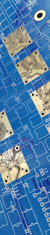
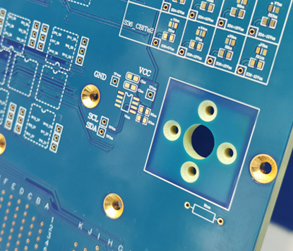
Backplane PCB
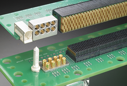
Backplane PCBs, also known as Interconnect Boards, are circuit boards designed to provide structural support and facilitate electrical connections between various components or modules in electronic systems, serving as central platforms for connecting multiple function boards like daughter boards or line cards while offering power distribution, signal transmission, and mechanical support to enable the overall functionality of the systems, and are commonly used in applications such as servers, telecommunications equipment, and large-scale computing systems. Backplane PCBs represent specialized forms of printed circuit board technology commonly employed in minicomputers and high-reliability applications. Functioning as arrays of electrical connectors arranged in parallel, each pin on the PCBs is linked to corresponding pins on all other connectors, forming interconnected internal systems. These arrangements serve as foundational frameworks for interconnecting multiple PCBs to form comprehensive systems. Interconnect Boards serve as central infrastructure components that facilitate the interconnection, communication, and power distribution within electronic systems. Their design considerations, such as signal integrity, scalability, reliability, and flexibility, play crucial roles in the overall functionality and performance of the interconnected systems. Key Characteristics of Backplane PCB : |
 |
|
 |
1, Interconnection: Backplane PCB’s primary function is to establish electrical connections between different modules, cards, or components within a system, typically featuring multiple slots, connectors, traces, and signal lines that enable communication and data transfer between the interconnected elements. 2, Scalability: Backplane PCBs are designed to support scalability and modularity in electronic systems. They allow for the easy addition or removal of expansion cards, modules, or components without requiring significant changes to the system architecture. This flexibility enables system upgrades, customization, and future expansion. 3, Form Factor: Backplane PCBs come in various form factors and configurations to accommodate different system requirements. They can be customized based on the specific needs of the application, such as the number of slots, types of connectors, and layout of signal lines. |
|
4, High-Speed Data Transmission: Backplane PCBs are engineered to support high-speed data transmission and communication protocols. They may incorporate advanced signal integrity features, controlled impedance traces, and shielding techniques to ensure reliable data transfer at high speeds without signal degradation or loss. 5, Power Distribution: In addition to data connections, Backplane PCBs often include power distribution lines to supply electrical power to the connected modules and components. Proper power management and distribution are essential for ensuring the reliable operation of the entire system. 6, Redundancy and Fault Tolerance: Some Backplane PCB designs incorporate redundancy and fault-tolerant features to enhance system reliability. Redundant power supplies, hot-swappable modules, and dual-redundant communication paths are examples of mechanisms used to minimize downtime and prevent system failures. |
||
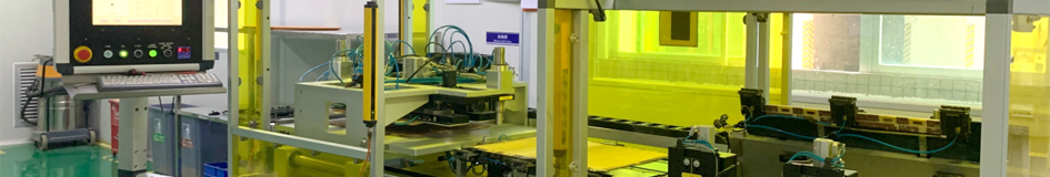
Manufacturing Challenges of Backplane PCB : |
1, PCB Thickness: 2, Back-Drilling: |
|
 |
3, Plating Aspect Ratio: 4, Connectors Alignment: |
5, Pressing Process: 6, Compliance and Standards: |
|
 |
7, Layer Registration: 8, Thermal Management: 9, Signal Integrity: |
10, Testing and Quality Assurance: 11, Cost Constraints: |
|
Advantages of Backplane PCB : |
1, Scalability: Backplane PCBs offer the flexibility to accommodate multiple slots or connectors, facilitating the addition of new components or system expansion without extensive modifications. This scalability feature makes backplane PCBs a cost-effective and scalable solution for electronic systems requiring future upgrades. 2, Streamlined Interconnectivity: Backplane PCBs simplify the assembly process, mitigate signal loss risks, and enhance overall system reliability. They enable straightforward interconnection between multiple circuit boards or modules, eliminating the need for multiple connectors and cables by serving as a centralized backbone. |
|
 |
3, Space Efficiency: Backplane PCBs prove especially beneficial for space-constrained systems or applications demanding high portability. By utilizing backplane PCBs, valuable space within the system is conserved, reducing the reliance on bulky and intricate cabling arrangements. 4, Enhanced Signal Integrity: Backplane PCBs establish a consistent and controlled environment for signal transmission, promoting improved signal integrity. By minimizing signal distortion, crosstalk, and electromagnetic interference, backplane PCBs help maintain the optimal performance of electronic systems. 5, Modular Design: Backplane PCBs enable a modular design approach, allowing for easier integration and replacement of individual modules or components. This modularity enhances flexibility in system configuration and maintenance, simplifying upgrades or repairs without requiring significant rework of the entire system. |
6, Signal Distribution: Backplane PCBs excel in distributing signals efficiently across multiple interconnected modules or boards within an electronic system. They provide a centralized platform for managing signal routing, reducing signal propagation delays and ensuring consistent signal quality throughout the system. 7, EMI Shielding: Backplane PCBs can incorporate effective electromagnetic interference (EMI) shielding measures to mitigate the impact of external electromagnetic disturbances on sensitive electronic components. By integrating shielding techniques into the backplane design, manufacturers can enhance system reliability and performance in electrically noisy environments. 8, High-Speed Data Transmission: Backplane PCBs are designed to support high-speed data transmission requirements in modern electronic systems. With optimized signal routing, impedance control, and signal integrity considerations, backplane PCBs facilitate reliable communication between interconnected modules at high data rates, essential for applications demanding rapid data transfer. |
|
Typical Applications of Backplane PCB : |
1, Telecommunications Systems: Backplane PCBs are commonly used in telecommunications infrastructure, such as network switches, routers, and communication servers. They facilitate the interconnection of multiple modules and boards, enabling efficient data transmission and signal distribution within complex telecommunications systems. |
|
 |
2, Industrial Automation: In industrial automation equipment like PLCs (Programmable Logic Controllers), SCADA systems, and industrial control units, backplane PCBs play a vital role in providing a centralized platform for connecting control modules, input/output devices, and communication interfaces. The modular design of backplane PCBs allows for flexible system configuration and expansion in industrial automation applications. 3, Data Centers and Servers: Backplane PCBs are essential components in data center servers and storage systems, where they serve as the backbone for connecting server blades, storage drives, and networking modules. By facilitating high-speed data transmission and signal integrity, backplane PCBs help optimize the performance and scalability of data center infrastructure. 4, Military and Aerospace Electronics: In military and aerospace applications, backplane PCBs are utilized in mission-critical systems such as radar systems, avionics equipment, and communication systems. The rugged design of backplane PCBs, along with their ability to withstand harsh environmental conditions and stringent reliability requirements, makes them ideal for use in defense and aerospace electronics. |
5, Medical Devices: Backplane PCBs play a crucial role in medical devices and equipment, including diagnostic instruments, patient monitoring systems, and medical imaging devices. They enable the integration of various electronic components and modules, ensuring reliable operation and data communication in healthcare applications. 6, Test and Measurement Instruments: Backplane PCBs are commonly employed in test and measurement equipment, such as oscilloscopes, spectrum analyzers, and signal generators. These PCBs provide a structured platform for connecting measurement modules and interface cards, facilitating accurate signal processing and data acquisition in test and measurement applications. |
|
Design Considerations for Backplane PCB : |
1, Pinout Definition: The initial step in designing a Backplane PCB is defining the pinout on the connectors to support the required routing topology effectively. 2, Mechanical Considerations: Alongside appropriately placing daughterboard connectors on the Backplane PCB, guide pins are essential for ensuring precise mating and structural integrity. 3, Material Selection: In high-speed Backplane PCB designs, material selection is a critical aspect. Given the potential size of backplanes, signals traversing the entire plane may suffer significant loss. Low-loss laminates with a tight glass weave are crucial to minimizing insertion loss on lengthy interconnects. |
|
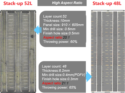 |
4, Power and Grounding Strategy: When dealing with Backplane PCBs that must distribute high power to numerous daughterboards, a well-defined power and grounding strategy is vital for maintaining low temperatures. The arrangement of ground and power planes on different layers of the Backplane PCB should also ensure isolation for high-speed signals routed across the board. 5, Layer Configuration: The number of layers required in a Backplane PCB depends on both the plane layer count and the quantity of signal layers needed. Backplane PCBs can feature up to 60 layers and be several millimeters thick to accommodate diverse design requirements effectively. 6, Signal Integrity: Maintaining signal integrity is crucial in Backplane PCB design, especially for high-speed data transmission applications. Factors such as controlled impedance routing, signal crosstalk mitigation, and proper termination techniques should be carefully considered to ensure reliable signal performance and minimize interference. |
7, Thermal Management: Efficient thermal management is essential for Backplane PCBs, particularly in systems handling high power levels or operating in demanding environments. Incorporating thermal vias, heat sinks, and proper airflow design can help dissipate heat effectively and prevent overheating of components on the board. 8, Compliance and Standards: Ensuring compliance with industry standards and regulations is imperative in Backplane PCB design. Adhering to standards such as IPC-2221 for PCB design, RoHS directives for environmental protection, and specific industry requirements helps guarantee the reliability, safety, and interoperability of the final product. 9, Testing and Verification: Thorough testing and verification procedures are essential during the design and manufacturing phases of Backplane PCBs. Performing signal integrity analysis, thermal simulations, and functional testing can help identify and resolve potential issues early in the development process, leading to a more robust and reliable product. |
|
Why Choose PANDA PCB for Interconnect Board ? |
 |
PANDA PCB, a seasoned industry leader with 20 years of experience specializing in high-end Main Board production. With a remarkable capacity of up to 60 layers, we offer unparalleled expertise and capabilities to meet the most demanding design requirements. ● Specialization: With a laser focus on Main Boards, we bring unmatched expertise and precision to every project. ● Cutting-Edge Technology: Our advanced manufacturing facilities boast state-of-the-art equipment, ensuring top-notch quality and performance. ● Customization: Tailored to your exact specifications, our Backplane PCBs are designed to meet your unique needs with precision and flexibility. ● Quality Assurance: Rigorous quality control measures at every stage guarantee reliability, accuracy, and consistency in all our products. |
|
● Industry Experience: With a proven track record spanning over a decade, our experienced team brings deep industry knowledge and insight to every project. Choose PANDA PCB for unrivaled expertise, cutting-edge technology, and a commitment to excellence in Backplane PCB manufacturing. Elevate your electronic systems with our high-quality solutions. |
|
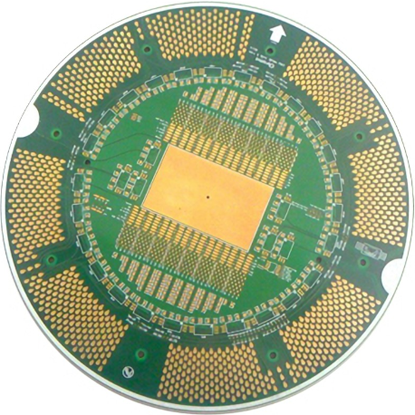
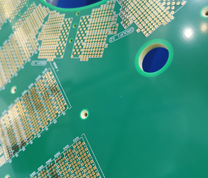
Capabilities of Backplane PCB : |
Appearance |
Standard |
High |
Advanced |
Layer Count (Max. Layers): |
16 |
40 |
60+ |
PCB Size (Max.): |
1100mm×500mm |
1200mm×550mm |
1200mm×630mm |
Thickness (Max.): |
8mm |
10mm |
15mm+ |
Outer Layer Line Width/Space: |
0.006"/0.006" |
0.005"/0.005" |
0.004"/0.004" |
Press-fit Hole Size Tolerance |
+/-2mil |
+/-2mil |
+2/-1mil |
Through Hole Aspect Ratio: |
14:1 |
17:1 |
20:1 |
Drill Registration: |
+/-5mil |
+/-4mil |
+/-3mil |
Buried Vias: |
Yes |
Yes |
Yes |
Blind Vias: |
Layers n to n-1 |
Layers n to n-2 |
Layers n to n-3 |